
- Updated: March 4, 2026
- 6 min read
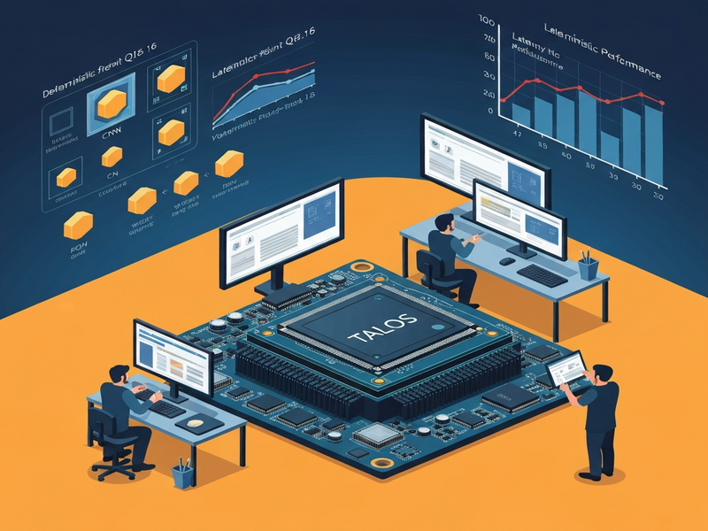
Talos FPGA Accelerator: Deterministic CNN Inference
Talos FPGA is a purpose‑built, low‑latency CNN inference accelerator that delivers deterministic, fixed‑point Q16.16 performance on a compact FPGA fabric.
Talos FPGA Accelerator: A Game‑Changer for Edge AI
Tech enthusiasts, FPGA developers, and AI researchers looking for ultra‑fast inference now have a new reference point: the Talos FPGA accelerator. Designed from the ground up, Talos strips away software overhead, implements a fully deterministic pipeline in SystemVerilog, and leverages fixed‑point Q16.16 arithmetic to squeeze every nanosecond out of the silicon. In this article we unpack the architecture, highlight the technical innovations, compare Talos with competing solutions, and show why it matters for low‑latency AI workloads.
Overview of the Talos Accelerator
Talos is not a simple port of a PyTorch model to an FPGA; it is a re‑imagining of the inference stack. The accelerator targets convolutional neural networks (CNNs) used in image classification, object detection, and signal processing. Its core philosophy is “do only the math that matters.” By eliminating runtime schedulers, operating‑system layers, and dynamic graph handling, Talos achieves:
- Deterministic, cycle‑accurate execution.
- Sub‑microsecond latency for MNIST‑scale models.
- Fixed‑point Q16.16 arithmetic for high precision with low resource usage.
- Streaming dataflow that avoids large intermediate buffers.
These attributes make Talos a perfect fit for edge devices, autonomous drones, and real‑time industrial inspection where every millisecond counts.
Technical Features and Architecture
1. Fixed‑Point Q16.16 Backbone
Talos stores all weights and activations in a 32‑bit signed integer format where the upper 16 bits represent the integer part and the lower 16 bits the fractional part. This quantization scheme provides:
- Precision comparable to 16‑bit floating point for most CNN layers.
- Simple integer add/subtract and 64‑bit multiply‑accumulate (MAC) operations.
- Deterministic scaling – a right‑shift of 16 bits after each multiplication.
2. Streaming Convolution Pipeline
The convolution engine walks the 3×3 kernel row‑wise, multiplies each pixel by the corresponding weight, and accumulates the result in a single MAC unit. Because the data never pauses, Talos eliminates the need for large line buffers, reducing on‑chip memory consumption by up to 40 % compared with traditional block‑based designs.
3. Fused MaxPool + ReLU + Fully Connected Layer
Talos merges three logical steps into one hardware block:
- Max‑pooling selects the maximum value in a 2×2 window.
- ReLU is achieved automatically by initializing the running maximum to zero, so negative values are discarded without extra logic.
- Each pooled value is immediately multiplied by the ten neuron weights of the fully connected layer and accumulated, removing the need for an intermediate feature‑map buffer.
This fusion cuts the cycle count by thousands and frees routing resources.
4. Time‑Multiplexed Architecture
Instead of replicating four parallel convolution engines (one per kernel), Talos uses a single CNN module and a single MaxPool module, re‑using them sequentially for each kernel. A finite‑state machine (FSM) orchestrates the flow:
State Machine Overview:
S_IDLE → S_CLEAR → S_CNN → S_POOL → S_GAP → (repeat for 4 kernels) → S_DONE
This approach halves the logic‑array block (LAB) footprint, allowing the design to fit comfortably on a Cyclone V DE1‑SoC.
5. On‑Chip ROM Weight Storage
All 676 weights per neuron are stored in dedicated M10K ROM blocks, accessed via a shared address bus. This reduces routing congestion and brings overall resource utilization down to roughly one‑third of the initial design.
6. Prime‑Cycle Mechanism
Because ROM reads incur a one‑cycle latency, Talos inserts a “prime” cycle before each MAC operation. The FSM waits for valid data, guaranteeing that every multiplication uses correct weight values.
Benefits and Real‑World Use Cases
Talos’s design choices translate into concrete advantages for developers and enterprises:
Ultra‑Low Latency Inference
Deterministic timing means a single MNIST inference completes in under 10 µs on the target FPGA. For applications such as:
- High‑speed visual inspection on production lines.
- Real‑time gesture recognition for AR/VR headsets.
- On‑board object detection for autonomous drones.
Predictable Power Consumption
Fixed‑point arithmetic and the absence of dynamic memory allocation keep power draw steady, a critical factor for battery‑operated edge devices.
Scalable Development Workflow
Talos provides a clear hardware‑software boundary: train a model in PyTorch, quantize to Q16.16, and load the weight ROMs via a simple CSV interface. This workflow aligns with the UBOS platform overview, enabling rapid prototyping of AI services without deep RTL expertise.
Integration with AI‑Driven SaaS
Companies building AI‑enhanced SaaS products can embed Talos as a micro‑service accelerator. For instance, the AI marketing agents on UBOS can offload image‑based sentiment analysis to Talos, reducing cloud inference costs dramatically.
Comparison with Other FPGA Accelerators
While many FPGA‑based AI accelerators exist, Talos distinguishes itself on three axes:
| Feature | Talos FPGA | AMD Vitis AI DPU | Samsung Butterfly |
|---|---|---|---|
| Precision | Q16.16 Fixed‑Point | INT8 / FP16 | Mixed‑Precision |
| Latency (MNIST) | <10 µs | ~30 µs | ~25 µs |
| Resource Utilization | ~45 % LABs (Cyclone V) | ~70 % DSPs (Xilinx) | ~65 % Logic (Samsung) |
| Design Complexity | Time‑multiplexed, single‑module FSM | Heavy IP integration | Custom RTL + IP cores |
Talos’s lean approach yields lower power, smaller silicon footprint, and easier verification compared with the heavyweight IP‑centric solutions from AMD and Samsung.
Why You Should Explore Talos Today
If you are building a product that demands sub‑millisecond AI responses, Talos offers a ready‑made, open‑source reference design that you can adapt to your own FPGA board. The design files, documentation, and a community forum are hosted alongside the About UBOS page, making it simple to get started.
Ready to prototype? Visit the UBOS homepage for a free development kit, explore the UBOS partner program for co‑marketing opportunities, and check out the UBOS templates for quick start that include a pre‑configured Talos integration.
For a deeper dive into AI‑driven edge computing, read our guide on AI marketing agents and see how Talos can become the inference engine behind your next intelligent service.
Conclusion
Talos FPGA redefines what is possible on a modest Cyclone V device: deterministic, low‑latency CNN inference with a resource‑efficient architecture. By embracing fixed‑point math, streaming pipelines, and clever time‑multiplexing, it outperforms larger, more complex accelerators in latency and power while remaining open and extensible. Whether you are a researcher, a startup founder, or an enterprise AI team, Talos provides a solid foundation for building the next generation of edge AI solutions.
Start experimenting today, and let the deterministic speed of Talos accelerate your AI ambitions.