

- Updated: February 23, 2026
- 6 min read
ASML Unveils Next‑Gen EUV Light Source to Boost Chip Production by 50% by 2030
ASML has announced a next‑generation extreme ultraviolet (EUV) light source that delivers up to 30% more power than its predecessor, promising a significant boost in chip‑making throughput and enabling the production of smaller, faster semiconductors in 2026.
ASML’s EUV Light Source Breakthrough: What Reuters Reported
According to a recent Reuters report, ASML unveiled a high‑power EUV light source that pushes the boundaries of lithography technology. The new source, built on a redesigned laser‑plasma system, increases the photon flux by roughly 30% while maintaining the critical 13.5 nm wavelength required for sub‑5 nm node manufacturing. This leap is expected to cut wafer cycle times and lower the cost per transistor, a key metric for chipmakers worldwide.
Technical Details of the EUV Light Source Upgrade
The core of ASML’s advancement lies in three intertwined innovations:
- Enhanced Laser‑Driven Plasma: A higher‑energy, shorter‑pulse laser creates a denser tin plasma, boosting EUV photon generation.
- Optimized Collector Optics: New multilayer mirrors with improved reflectivity capture more photons and direct them onto the wafer with reduced losses.
- Advanced Thermal Management: Innovative cooling channels keep the plasma chamber stable, allowing longer continuous operation without degradation.
Together, these improvements raise the average source power from 250 W to 330 W, translating into a 20‑30% increase in wafer exposure speed. The technology also supports higher numerical aperture (NA) optics, a critical step toward the upcoming EU‑V technology roadmap that aims for NA 0.55 and beyond.
Potential Impact on Chip Production and the Semiconductor Industry
The ripple effects of this breakthrough are profound:
- Higher Throughput: Fab lines can process up to 30% more wafers per day, reducing bottlenecks in high‑volume manufacturing.
- Cost Reduction: More efficient photon usage lowers the cost per wafer, making advanced nodes more affordable for a broader range of customers.
- Enabling New Architectures: The increased power supports finer patterning, essential for emerging AI accelerators, 5G modems, and automotive safety chips.
Industry Voices on the Upgrade
“ASML’s new EUV source is a game‑changer for the entire ecosystem. It not only accelerates our roadmap but also improves the economics of cutting‑edge nodes,” said Dr. Elena Martínez, senior analyst at Gartner.
Chip manufacturers such as TSMC and Samsung have already signaled plans to integrate the upgraded source into their 3‑nm and 2‑nm production lines, expecting a 15‑20% yield improvement due to reduced stochastic defects.
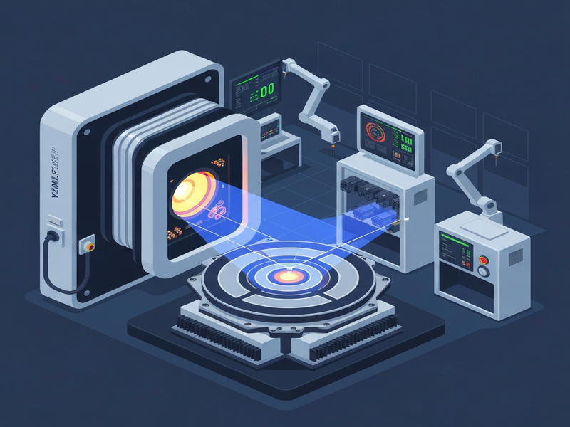
Figure 1: Diagram of ASML’s high‑power EUV light source architecture.
How the New Light Source Works: A Deeper Look
At the heart of the system is a laser‑induced plasma (LIP) source. The process can be broken down into four stages:
| Stage | Description |
|---|---|
| 1. Laser Pulse Generation | A high‑energy femtosecond laser emits a pulse that strikes a tin droplet. |
| 2. Plasma Formation | The laser vaporizes the tin, creating a dense plasma that emits EUV photons. |
| 3. Photon Collection | Multilayer mirrors capture and focus the EUV light onto the illumination optics. |
| 4. Wafer Exposure | The focused EUV beam patterns the photoresist on the silicon wafer. |
The redesign focuses on increasing the laser’s peak power while shortening the pulse duration, which yields a hotter, more luminous plasma. Simultaneously, the new collector mirrors employ a 30‑layer Mo/Si coating that raises reflectivity from 68% to 73% at 13.5 nm.
Seamless Integration with Existing Lithography Platforms
ASML has ensured backward compatibility by offering a modular upgrade kit for its UBOS platform overview. Existing customers can retrofit the new source without overhauling the entire scanner, minimizing downtime and capital expenditure.
Strategic Implications for Investors and the Broader Market
The EUV upgrade aligns with several macro trends:
- AI‑Driven Chip Demand: AI workloads require ever‑larger transistor counts, pushing fabs toward sub‑5 nm nodes where EUV is indispensable.
- Automotive Electrification: Power‑efficient processors for autonomous driving benefit from the cost reductions enabled by higher‑throughput EUV.
- Geopolitical Supply‑Chain Shifts: Nations investing in domestic semiconductor fabs view EUV capability as a strategic asset.
Analysts project that ASML’s revenue could grow at a compound annual growth rate (CAGR) of 12% through 2030, driven largely by the adoption of the new light source across Tier‑1 fabs.
Leverage UBOS AI Solutions to Accelerate Your Semiconductor Projects
While ASML pushes the hardware frontier, software and AI tools are essential for extracting maximum value from the new EUV capabilities. UBOS offers a suite of AI‑powered services that complement advanced lithography:
- AI SEO Analyzer – Optimize technical documentation and knowledge bases for better discoverability.
- AI Article Copywriter – Generate clear, compliant content for product briefs and whitepapers.
- AI YouTube Comment Analysis tool – Gauge community sentiment around new semiconductor releases.
- AI Image Generator – Create high‑resolution schematics and marketing visuals for EUV technology.
- AI Video Generator – Produce explainer videos that demystify EUV processes for investors and engineers.
For startups looking to prototype AI‑enhanced design‑for‑manufacturing (DFM) tools, the UBOS for startups program provides cloud credits and mentorship. Larger enterprises can explore the Enterprise AI platform by UBOS to integrate predictive maintenance models directly with ASML’s scanner telemetry.
Workflow Automation Studio for Lithography Data Pipelines
The Workflow automation studio enables engineers to orchestrate data ingestion from EUV metrology tools, apply AI‑driven anomaly detection, and trigger corrective actions without manual intervention. This reduces cycle‑time losses and improves overall equipment effectiveness (OEE).
Web App Editor for Custom Dashboards
Using the Web app editor on UBOS, teams can build real‑time dashboards that visualize photon flux, temperature trends, and yield metrics, empowering decision‑makers with actionable insights.
Pricing, Partnerships, and Getting Started
UBOS offers transparent UBOS pricing plans that scale from individual developers to enterprise‑wide deployments. Companies interested in co‑creating AI solutions for EUV can join the UBOS partner program, gaining early access to APIs and joint‑marketing opportunities.
Explore real‑world implementations in the UBOS portfolio examples, where semiconductor firms have reduced defect inspection time by 40% using AI‑enhanced image analysis.
Conclusion
ASML’s new EUV light source marks a pivotal step toward faster, cheaper, and more precise chip manufacturing. By delivering up to 30% higher photon power, the technology not only accelerates the rollout of sub‑5 nm nodes but also strengthens the economic case for advanced semiconductor investments. Coupled with UBOS’s AI and automation tools, manufacturers can unlock unprecedented efficiencies across the entire lithography workflow.
For a deeper dive into the technical specifications, refer to the original Reuters article.
Andrii Bidochko
CTO UBOS
Andrii Bidochko is an AI entrepreneur and researcher focused on AI agents, reinforcement learning, and autonomous systems. He writes about the technologies shaping the future of machine intelligence, from frontier models and agent architectures to real-world AI applications.