
- Updated: January 6, 2026
- 7 min read
Nvidia Partners with Siemens to Accelerate Chip Design Using GPUs
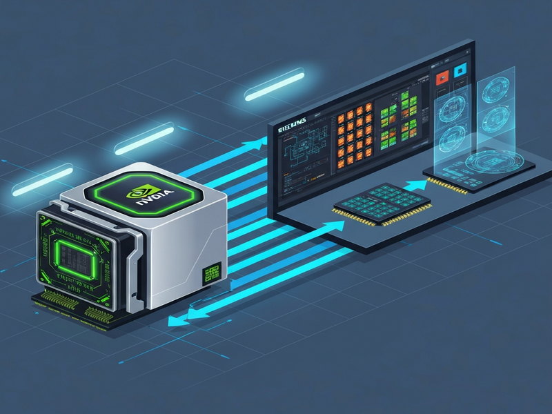
Nvidia is partnering with Siemens to accelerate Siemens’ electronic design automation (EDA) tools using Nvidia GPUs, a collaboration announced at CES 2026 that promises to dramatically shorten chip‑design cycles and enable high‑fidelity digital twins of semiconductor devices.
Nvidia‑Siemens Alliance: GPU‑Powered Chip Design Takes Center Stage at CES 2026
At the opening day of the Consumer Electronics Show 2026 in Las Vegas, Nvidia unveiled a strategic partnership with Siemens Digital Industries Software to port Siemens’ flagship EDA suite onto Nvidia’s latest GPU architecture. The move is positioned as a response to the exploding complexity of modern semiconductor designs, where billions of transistors must be simulated, verified, and optimized within ever‑shrinking timeframes.
By leveraging the parallel processing power of Nvidia GPUs, Siemens aims to cut design‑iteration times by up to 70 %, while simultaneously laying the groundwork for “digital twins” that replicate entire chips—or even full data‑center racks—in a virtual environment before silicon ever leaves the fab.
Partnership Details: How Nvidia GPUs Supercharge Siemens’ EDA Stack
The collaboration focuses on three core deliverables:
- GPU‑Optimized Kernels: Critical simulation kernels in Siemens’ Mentor Graphics suite are being rewritten in CUDA to exploit massive parallelism.
- Unified Development Environment: Engineers will access GPU‑accelerated workflows directly from Siemens’ existing UI, preserving familiar design‑entry paradigms.
- Digital Twin Framework: A new module will generate high‑resolution, physics‑based twins of chips, enabling early‑stage performance validation.
According to Nvidia CEO Jensen Huang, “Our GPUs are the only commodity hardware that can deliver the compute density required for next‑generation chip verification. By integrating with Siemens, we’re turning design bottlenecks into opportunities for rapid innovation.”
Siemens’ CTO, Dr. Anja Müller, added, “The partnership aligns with our vision of a fully virtualized semiconductor pipeline. GPU acceleration not only speeds up simulation but also opens the door to AI‑driven optimization that was previously infeasible.”
Why GPU Acceleration Matters for Semiconductor Design
GPU acceleration brings several tangible benefits to the EDA workflow:
1. Massive Parallelism Reduces Runtime
Traditional CPU‑bound simulations run sequentially, limiting throughput. Nvidia’s Ampere‑based GPUs can execute thousands of threads concurrently, turning hours‑long Monte‑Carlo analyses into minutes‑long tasks.
2. Energy Efficiency at Scale
GPUs deliver higher FLOPS per watt compared with CPU clusters, lowering operational costs for large design houses and cloud‑based EDA services.
3. Enabling AI‑Assisted Design
With GPU‑ready deep‑learning frameworks, designers can now embed generative AI models that suggest layout optimizations, predict failure points, and auto‑tune power‑performance trade‑offs.
4. Seamless Integration with Digital Twins
The new digital twin module leverages GPU‑accelerated physics engines to simulate thermal, electrical, and mechanical behavior in real time, providing a “what‑if” sandbox for design validation.
“GPU‑driven digital twins will let us test a chip’s behavior under extreme conditions before the first wafer is ever fabricated.” – Dr. Anja Müller
CES 2026 Highlights: The Announcement in Context
The unveiling took place during Siemens’ keynote, which also showcased a prototype of a fully virtualized data‑center rack powered by Nvidia GPUs. Attendees witnessed a live demonstration where a complex system‑on‑chip (SoC) design, previously taking 48 hours to verify, completed a full verification cycle in under 12 hours.
Industry analysts at the show noted that this partnership could reshape the competitive landscape of EDA, traditionally dominated by a few legacy vendors. By marrying Nvidia’s GPU leadership with Siemens’ deep domain expertise, the alliance creates a compelling alternative for semiconductor firms seeking faster time‑to‑market.
In a side interview, Jensen Huang referenced the “Vera Rubin” project—a future digital twin of a next‑generation GPU that will serve as a benchmark for AI‑driven chip design. The name pays homage to the famed astronomer Vera Rubin, symbolizing the quest to “see the unseen” in silicon.
Industry Implications: From Faster Time‑to‑Market to Full‑Scale Digital Twins
The ripple effects of this partnership extend beyond pure performance gains:
- Accelerated Innovation Cycles: Companies can iterate designs more rapidly, reducing the risk of costly mask re‑spins.
- Cost Reduction: Shorter simulation times translate into lower cloud‑compute bills and fewer engineering‑hour expenditures.
- Enhanced Collaboration: Cloud‑based GPU clusters enable geographically dispersed teams to work on the same digital twin in real time.
- New Business Models: SaaS‑style EDA offerings can now price GPU‑accelerated simulation as a consumable service, opening revenue streams for both Nvidia and Siemens.
For technology professionals, the move signals a shift toward AI‑first design methodologies. As AI models become integral to layout synthesis and verification, the underlying hardware must keep pace—something Nvidia’s GPUs are uniquely positioned to deliver.
What This Means for Your AI‑Powered Projects
If you’re exploring how GPU acceleration can transform your own workflows, consider the broader ecosystem that UBOS offers for AI‑driven development:
- Start with the UBOS homepage to explore a unified AI platform that supports GPU‑intensive workloads.
- Get a high‑level view of the UBOS platform overview, which includes native support for GPU‑accelerated inference.
- Leverage the Enterprise AI platform by UBOS to scale your chip‑design simulations across multiple GPU nodes.
- Accelerate your marketing analytics with AI marketing agents that can ingest simulation data and generate actionable insights.
- Join the UBOS partner program to co‑develop custom GPU‑enabled tools for your organization.
- Explore flexible pricing through the UBOS pricing plans, which include GPU‑compute credits.
- Kick‑start your next project with UBOS templates for quick start, such as the AI SEO Analyzer or the AI Article Copywriter.
- See real‑world implementations in the UBOS portfolio examples, which showcase GPU‑accelerated analytics pipelines.
- For startups, the UBOS for startups program offers credits and mentorship to embed GPU‑driven AI from day one.
- SMBs can benefit from UBOS solutions for SMBs, delivering enterprise‑grade GPU performance at a fraction of the cost.
- Build custom web interfaces with the Web app editor on UBOS, perfect for visualizing digital twins.
- Automate complex workflows using the Workflow automation studio, which can orchestrate GPU jobs, data ingestion, and result reporting.
- Integrate conversational AI into your design review process with the ChatGPT and Telegram integration or the OpenAI ChatGPT integration.
- Enhance data retrieval with the Chroma DB integration, enabling vector‑search over simulation results.
- Add lifelike voice feedback to your verification dashboards using the ElevenLabs AI voice integration.
- Finally, connect directly to Telegram for instant alerts via the Telegram integration on UBOS.
These resources illustrate how a modern AI‑centric stack can complement Nvidia’s GPU acceleration, giving you a full‑stack solution from data ingestion to actionable insight.
Read the Full Story
For a deeper dive into the announcement, see the original TechCrunch article.
Conclusion: A New Era for Chip Design
The Nvidia‑Siemens partnership marks a pivotal moment where high‑performance GPU computing meets the most demanding challenges of semiconductor design. By slashing simulation times, enabling AI‑driven optimization, and laying the foundation for comprehensive digital twins, the collaboration promises to accelerate innovation across the entire electronics ecosystem.
For engineers, executives, and AI enthusiasts alike, the message is clear: embracing GPU‑accelerated EDA is no longer optional—it’s a strategic imperative. Leveraging platforms like UBOS can further amplify these gains, providing a seamless bridge between raw compute power and intelligent, end‑to‑end workflows.
Stay ahead of the curve, explore the resources above, and consider how GPU‑powered AI can transform your next silicon project.